Printed circuit boards or, as they are commonly known, PCBs are prime components in every modern electronic gadget. These are the complex green pieces of plastic that have circuitry markings over it. You can find it inside your phone or your calculator. Undermining them would be a foolish mistake. These tiny apparatus are capable of performing complex tasks like controlling an aircraft. These components are either used singly or in combination, depending upon their application.
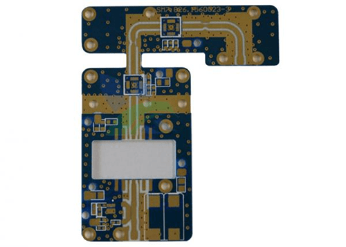
A PCB Consists of four layers that complete the pcb assembly. These four layers are:
- Substrate
- Copper layer
- Solder mask
- Silkscreen
Now that you’ve come to know what are the parts of a PCB, let’s move to the process. The steps to manufacturing a PCB are as below:
1. Designing and Printing The PCB
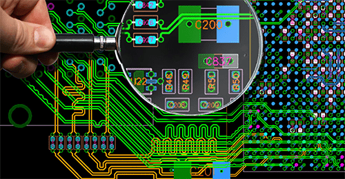
PCB manufacturer and the customer work closely in order to determine the requirements it needs to fulfill. A pcb design company may make use of designing software to design what the PCB should look like. Once the design is ready, it is printed in the form of a thin clear plastic sheet that has ink markings over it.
2. Printing The Copper For Interior
The ink markings on the plastic sheet mark the places where the copper is to be printed and where the components are to be placed. Copper has very low resistance and is widely preferred where high conductivity is needed.
3. Inspection And Layer Alignment
When all the different plastic layers (PCB) are printed, they are layered and aligned. An optical inspection and punching machine is used to layer the PCBs together so that there are no defects. The optical inspection machine ensures that all the layers are properly aligned.
4. Laminating The PCB Layer
A pair of heated press plates is used to combine the layers of PCB. the layers are either pre-soaked in an epoxy resin or are wrapped inside a pre-impregnated layer of epoxy film. The heat from the press melts the epoxy and fuses the layers together.
5. Drilling And PCB Plating
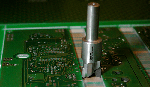
Once lamination is done, the assembled PCB is drilled to get holes to secure it on the mainframe. Finally, the drilled PCB is bathed in a series of chemicals to clean it. At the end of this process, a micro-layer of copper is plated over the top layer and into the holes of the PCB.
6. Applying The Solder Mask
Solder masks are thin preventive layers to protect the PCB from oxidation and forming any solder bridges between closely placed solder pads.
7. Cutting And Profiling
After the PCB is constructed it has to be separated from its construction panel. There could be more than one type of PCBs printed together onto one construction panel. They can either be cut off using CNC machines or Laser guided cutters or mechanically, with the help of initial design. Profiling of the PCBs is carried out to smoothen their ends and edges.
Whether you are working on a school project or you are a geek, you can easily construct your master PCB with the help of these steps.


