


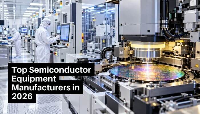

Semiconductor equipment manufacturers build the highly specialized machines that make modern chips possible. Before an AI accelerator, smartphone processor, memory chip, automotive semiconductor, or sensor reaches a finished product, specialized equipment must pattern microscopic circuits, deposit ultra-thin materials, remove unwanted layers, clean wafers, inspect defects, connect dies, and test the completed device.
The semiconductor equipment market is expanding quickly in 2026. SEMI forecasts worldwide semiconductor manufacturing equipment sales of $165.9 billion, up 23.2% year over year. Wafer-fab equipment, advanced memory, semiconductor testing, and packaging are benefiting from investment in AI computing, 2nm logic, high-bandwidth memory, 3D NAND, and increasingly complex chip architectures.
Leading suppliers include ASML, Applied Materials, Lam Research, Tokyo Electron, KLA, ASM International, SCREEN Holdings, Advantest, and Teradyne. Specialist companies such as Besi, DISCO, Canon, and Nikon also supply critical technologies used at different stages of semiconductor production.
This guide compares the leading semiconductor equipment manufacturers, explains what each company specializes in, examines the technologies driving demand in 2026, and explores the semiconductor equipment market outlook through 2028.
Quick Answer
The leading semiconductor equipment manufacturers in 2026 include ASML, Applied Materials, Lam Research, Tokyo Electron, KLA, ASM International, SCREEN Holdings, Advantest, and Teradyne.
However, there is no single company that makes every machine required to manufacture a semiconductor.
ASML is critical in advanced lithography. Applied Materials, Lam Research, and Tokyo Electron participate across major wafer-processing steps. KLA specializes in inspection and process control. ASM is strong in atomic layer deposition, while SCREEN is an important wafer-cleaning supplier. Advantest and Teradyne provide semiconductor testing systems.
Specialist companies including Besi, DISCO, Canon, and Nikon add important technologies in hybrid bonding, wafer grinding and dicing, conventional lithography, nanoimprint development, and advanced-packaging lithography.
Key Takeaways
- Global semiconductor manufacturing equipment sales are forecast to reach $165.9 billion in 2026, up 23.2%.
- Wafer-fab equipment sales are projected at $143.9 billion.
- Foundry and logic equipment sales are forecast at $78 billion.
- DRAM equipment sales are expected to reach $38.8 billion, supported partly by HBM investment.
- NAND equipment is projected at $13.9 billion.
- Semiconductor test equipment is forecast to grow 31% to $15.3 billion.
- High-NA EUV, gate-all-around transistors, HBM, 3D NAND, chiplets, and advanced packaging are major technology drivers.
- China, Taiwan, and South Korea are expected to remain the three largest equipment-spending destinations through 2028.
- SEMI forecasts worldwide semiconductor equipment sales reaching approximately $229.5 billion in 2028.
What Are Semiconductor Equipment Manufacturers?
Semiconductor equipment manufacturers develop and produce the specialized machinery used to fabricate, inspect, package, and test integrated circuits.
Their customers include:
- Semiconductor foundries
- Integrated device manufacturers
- Memory manufacturers
- Specialty semiconductor fabs
- Outsourced semiconductor assembly and test (OSAT) companies
- Semiconductor research and development facilities
A chip does not pass through a single machine before it is completed. Instead, a semiconductor wafer may undergo hundreds or even thousands of individual process steps before finished dies are ready for packaging.
Materials must be deposited onto the wafer, while lithography systems create microscopic circuit patterns. Etching removes selected materials, ion implantation changes electrical properties, cleaning eliminates microscopic contamination, and chemical mechanical polishing creates extremely flat wafer surfaces.
Inspection and metrology systems repeatedly check whether these processes remain within the tight tolerances required for reliable semiconductor production.
After wafer fabrication, additional equipment thins and cuts the wafer, separates individual dies, bonds components together, creates advanced packages, and tests whether the finished devices operate correctly.
Because each manufacturing stage requires different technologies and extremely high precision, semiconductor equipment manufacturers often specialize in particular processes rather than attempting to supply every machine used in chip production. This specialization is why the industry includes major suppliers alongside smaller companies that lead individual equipment categories.
Main Types of Semiconductor Manufacturing Equipment
| Equipment Type | Primary Function | Major Manufacturers |
|---|---|---|
| Lithography | Transfers circuit patterns onto wafers | ASML, Canon, Nikon |
| Thin-film deposition | Deposits extremely thin material layers | Applied Materials, ASM, Lam Research, Tokyo Electron |
| Etching | Removes selected wafer materials | Lam Research, Tokyo Electron, Applied Materials |
| Wafer cleaning | Removes particles and residues | SCREEN, Tokyo Electron |
| CMP | Creates extremely flat wafer surfaces | Applied Materials, EBARA |
| Ion implantation | Introduces controlled dopants | Axcelis, Applied Materials |
| Inspection | Detects defects | KLA, Onto Innovation |
| Metrology | Measures dimensions and process variation | KLA, Onto Innovation, ASML |
| Wafer grinding | Reduces wafer thickness | DISCO |
| Wafer dicing | Separates individual dies | DISCO |
| Die bonding | Connects semiconductor dies | Besi |
| Advanced packaging | Integrates multiple dies and chiplets | Besi, Applied Materials, Tokyo Electron and others |
| Semiconductor testing | Tests device performance and reliability | Advantest, Teradyne |
This specialization is important when comparing semiconductor equipment manufacturers. A company with lower total revenue may still control a highly valuable manufacturing step.
Front-End vs. Back-End Semiconductor Equipment
Semiconductor production is commonly divided into front-end and back-end manufacturing, with different equipment required at each stage.
Front-End Semiconductor Manufacturing
Front-end processing creates the electronic structures directly on a semiconductor wafer. This stage includes many of the most precise and capital-intensive processes in chip production.
Important front-end processes include:
- Lithography
- Thin-film deposition
- Plasma etching
- Ion implantation
- Thermal processing
- Wafer cleaning
- Chemical mechanical polishing (CMP)
- Inspection
- Metrology
ASML, Applied Materials, Lam Research, Tokyo Electron, KLA, ASM International, and SCREEN Holdings are strongly associated with these manufacturing stages.
Back-End Semiconductor Manufacturing
Back-end manufacturing takes place after most wafer fabrication is complete. It focuses on preparing individual dies, integrating them into packages, and verifying that the finished semiconductor devices operate correctly.
Important back-end processes include:
- Wafer thinning
- Wafer dicing
- Die bonding
- Hybrid bonding
- Package assembly
- Advanced packaging
- Package inspection
- Semiconductor testing
Besi, DISCO, Advantest, and Teradyne have important positions across these areas.
The distinction between front-end and back-end manufacturing is becoming less rigid as advanced packaging grows more sophisticated. Technologies such as HBM, chiplets, and 3D integration increasingly require high-precision deposition, lithography, CMP, bonding, inspection, and metrology.
As a result, semiconductor equipment manufacturers that traditionally focused on front-end wafer fabrication are increasingly finding opportunities in advanced packaging and other back-end processes.
How Big Is the Semiconductor Equipment Market in 2026?
SEMI’s July 2026 forecast points to strong growth across multiple semiconductor equipment segments, supported by investment in AI infrastructure, advanced logic, memory, packaging, and testing.
| Market Segment | 2026 Forecast | Year-Over-Year Growth |
|---|---|---|
| Total semiconductor equipment | $165.9 billion | 23.2% |
| Wafer-fab equipment | $143.9 billion | 23.1% |
| Foundry and logic WFE | $78.0 billion | 18.9% |
| DRAM equipment | $38.8 billion | 39.0% |
| NAND equipment | $13.9 billion | 30.7% |
| Semiconductor test equipment | $15.3 billion | 31.0% |
| Assembly and packaging equipment | $6.7 billion | 9.6% |
The forecast shows that growth is not limited to one part of chip production. Leading-edge logic, HBM-related DRAM, NAND, semiconductor testing, and advanced packaging are all contributing to equipment demand.
AI is an especially important driver because an advanced AI accelerator requires more than the processor itself. It also depends on high-bandwidth memory, sophisticated packaging, interconnect technologies, process control, inspection, and extensive testing.
This creates opportunities for semiconductor equipment manufacturers across multiple stages of the production chain rather than only companies supplying machines for advanced logic fabrication.
Why the $165.9 Billion and $149 Billion Estimates Are Different
Readers researching the semiconductor equipment market may encounter two major 2026 figures: $165.9 billion and $149 billion. Although they may appear contradictory, they measure different parts of the industry.
SEMI’s $165.9 billion forecast represents worldwide semiconductor manufacturing equipment sales across the broader market, including wafer-fab, test, assembly, and packaging equipment.
By comparison, SEMI’s 300mm Fab Outlook projects approximately $149 billion in 300mm front-end fab equipment spending in 2026, up 31% year over year. This figure focuses specifically on equipment spending for 300mm front-end fabrication facilities rather than the entire semiconductor equipment market.
The distinction matters when evaluating market growth and opportunities for semiconductor equipment manufacturers. The $165.9 billion and $149 billion estimates come from different market definitions, so they should not be treated as competing forecasts of the same equipment category.
Top Semiconductor Equipment Manufacturers in 2026
The leading semiconductor equipment manufacturers serve different stages of chip production, from lithography and wafer processing to inspection, cleaning, advanced packaging, and final testing. No single supplier dominates every manufacturing step.
| Company | Headquarters | Best Known For |
|---|---|---|
| ASML | Netherlands | EUV and DUV lithography |
| Applied Materials | United States | Deposition, materials engineering, CMP, etch |
| Lam Research | United States | Etch, deposition and wafer processing |
| Tokyo Electron | Japan | Etch, coat/develop, deposition and cleaning |
| KLA | United States | Inspection, metrology and process control |
| ASM International | Netherlands | Atomic layer deposition and epitaxy |
| SCREEN Holdings | Japan | Wafer cleaning |
| Advantest | Japan | Semiconductor testing |
| Teradyne | United States | Automated semiconductor testing |
| Besi | Netherlands | Assembly and hybrid bonding |
| DISCO | Japan | Wafer grinding and dicing |
| Canon | Japan | Semiconductor lithography and nanoimprint |
| Nikon | Japan | Lithography and advanced packaging |
Methodology note: The companies are included based on their technological importance, product specialization, industry scale, and relevance to major semiconductor manufacturing processes. This is not a strict revenue ranking because fiscal periods, currencies, equipment categories, and business mixes differ.
1. ASML
ASML is one of the most strategically important semiconductor equipment manufacturers because of its position in advanced lithography.
The company reported €32.7 billion in total net sales in 2025, including €24.5 billion from systems and €8.2 billion from services and field options. It shipped 48 EUV systems, 279 DUV systems, and 208 metrology and inspection systems during the year.
ASML’s importance is closely tied to extreme ultraviolet (EUV) lithography, which enables patterning for leading-edge chips. Its next-generation High-NA EUV technology is designed to extend advanced patterning further. In September 2026, ASML and Intel Foundry reported that High-NA systems had processed more than one million wafers across qualification, development, research, and selected production activities.
2. Applied Materials
Applied Materials has one of the industry’s broadest equipment portfolios, covering deposition, etching, CMP, epitaxy, ion implantation, materials engineering, inspection, and advanced packaging.
In June 2026, the company introduced new technologies aimed at advanced DRAM, HBM, and AI-related packaging, including epitaxy, deposition, CMP, and electron-beam systems.
Applied Materials is particularly well positioned for manufacturing transitions that require new materials and additional process steps, including gate-all-around transistors, backside power delivery, HBM, hybrid bonding, and chiplets.
3. Lam Research
Lam Research is a major supplier of semiconductor etching, deposition, cleaning, and wafer-processing equipment.
The company generated approximately $23.23 billion in fiscal 2026 revenue, compared with $18.44 billion in fiscal 2025, while research and development spending reached about $2.38 billion.
Lam’s technologies are especially relevant to complex three-dimensional structures. Higher-layer 3D NAND, GAA transistors, advanced memory, and increasingly complicated interconnects require highly controlled material deposition and removal.
4. Tokyo Electron
Tokyo Electron, commonly known as TEL, supplies equipment across multiple semiconductor processes, including coat/develop, plasma etch, deposition, thermal processing, wafer cleaning, probing, and bonding.
The company reported ¥2.4435 trillion in semiconductor production equipment sales for fiscal 2026.
TEL’s broad portfolio gives it exposure to logic, memory, and advanced packaging rather than making it dependent on one manufacturing process.
5. KLA
KLA specializes in semiconductor inspection, metrology, process control, and yield management.
The company reported approximately $13.58 billion in fiscal 2026 revenue, including roughly $12.24 billion from semiconductor process control. Wafer inspection represented about 49% of total revenue, while services accounted for approximately 23%.
KLA’s technologies become increasingly valuable as semiconductor structures shrink and manufacturing costs rise. Advanced logic, EUV, HBM, chiplets, and complex packages all require precise defect detection and process measurement.
6. ASM International
ASM International specializes in semiconductor deposition, particularly atomic layer deposition (ALD) and epitaxy.
The company reported record 2025 revenue of approximately €3.2 billion, with advanced logic and foundry investment contributing to growth as customers expanded 2nm gate-all-around capacity.
ALD is particularly valuable for modern three-dimensional transistor structures because it can create extremely thin and uniform films across complicated surfaces.
7. SCREEN Holdings
SCREEN Holdings is an important supplier of semiconductor wafer-cleaning equipment, including single-wafer cleaning systems, batch cleaning equipment, and spin scrubbers.
The company reported consolidated sales of ¥605.7 billion for the fiscal year ended March 31, 2026.
Wafer cleaning remains essential because microscopic particles and chemical residues can damage advanced semiconductor structures and reduce manufacturing yield.
8. Advantest
Advantest is one of the world’s major semiconductor test-equipment suppliers.
In July 2026, the company raised its fiscal 2026 sales forecast to ¥1.714 trillion, citing strong demand connected to increasing production and complexity of AI-related semiconductors.
AI accelerators, advanced memory, and increasingly complex packages require more extensive testing, strengthening demand for sophisticated automated test equipment.
9. Teradyne
Teradyne is another major supplier of automated semiconductor testing systems.
Its Q2 2026 revenue reached $1.329 billion, including approximately $1.122 billion from Semiconductor Test. Semiconductor Test revenue increased 128.1% year over year, primarily because of stronger AI-related compute and memory demand.
Together, these leading semiconductor equipment manufacturers demonstrate how AI investment is spreading across the entire chip-production ecosystem—from lithography and wafer processing to process control and final device testing.
Other Important Semiconductor Equipment Manufacturers
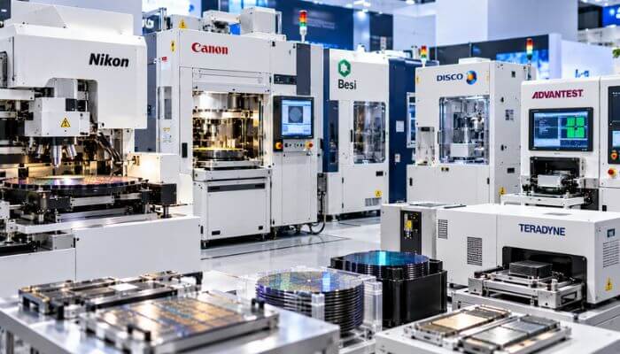
Beyond the largest suppliers, several specialist semiconductor equipment manufacturers hold important positions in hybrid bonding, wafer processing, lithography, and advanced packaging.
Besi: Hybrid Bonding and Assembly
BE Semiconductor Industries, commonly known as Besi, develops semiconductor assembly and packaging equipment, with growing exposure to hybrid bonding for HBM, chiplets, AI accelerators, photonics, and 3D integration.
Besi generated €434.7 million in revenue during the first half of 2026, up 48.8% year over year, while orders increased 116.5%. The company highlighted demand related to hybrid bonding, photonics, data-center computing, and AI applications.
DISCO: Wafer Grinding and Dicing
DISCO specializes in precision wafer processing, including grinding, blade dicing, laser dicing, and surface processing.
In February 2026, cumulative shipments of DISCO laser saws exceeded 4,000 systems. Its technologies are increasingly relevant as advanced memory and packaging require thinner dies and highly precise, low-damage wafer processing.
Canon: Lithography and Nanoimprint
Canon remains an important supplier of semiconductor lithography equipment outside the advanced EUV market.
The company projected 238 semiconductor lithography system shipments in 2026, including 69 KrF and 169 i-line systems.
Canon is also developing nanoimprint lithography, which transfers circuit patterns using a physical template. The technology is being evaluated for potential production applications, although its adoption will depend on defect control, overlay accuracy, throughput, economics, and specific manufacturing requirements.
Nikon: Lithography and Advanced Packaging
Nikon supplies semiconductor lithography equipment and is expanding its exposure to advanced packaging.
Its DSP-100 digital lithography system supports substrates up to 600 × 600 mm, with 1.0 µm line-and-space resolution and stated throughput of 50 panels per hour under specified conditions.
Nikon’s expansion into packaging illustrates a broader trend among semiconductor equipment manufacturers: technologies traditionally associated with front-end wafer fabrication are increasingly being adapted for advanced packaging and chip integration.
Technologies Driving Semiconductor Equipment Demand in 2026
Several technology transitions are increasing demand for semiconductor equipment manufacturers across wafer fabrication, process control, packaging, and testing.
1. High-NA EUV Lithography
High-NA EUV is designed to improve patterning capability for increasingly small chip features. In September 2026, Intel Foundry and ASML reported that High-NA systems had processed more than one million wafers across qualification, R&D, and selected production activities.
Its adoption can also increase requirements for masks, etching, deposition, inspection, and metrology.
2. Gate-All-Around Transistors
Gate-all-around (GAA) transistors use nanosheet structures to support continued transistor scaling but require more complex manufacturing.
Their production increases the need for precise etching, atomic-scale deposition, epitaxy, cleaning, and metrology.
3. High-Bandwidth Memory
High-bandwidth memory (HBM) stacks DRAM dies to provide the high memory bandwidth required by many AI accelerators.
SEMI forecasts DRAM equipment sales rising 39% to $38.8 billion in 2026. HBM also drives demand for wafer thinning, bonding, advanced packaging, inspection, and testing equipment.
4. 3D NAND
3D NAND increases storage density by stacking memory layers vertically. As these structures become taller, manufacturers need increasingly precise etching, deposition, cleaning, inspection, and metrology.
SEMI forecasts NAND equipment sales increasing 30.7% to $13.9 billion in 2026.
5. Advanced Packaging and Chiplets
Advanced packaging allows CPUs, AI accelerators, HBM, I/O dies, and other chiplets to be integrated within sophisticated packages.
This transition is creating additional opportunities for semiconductor equipment manufacturers supplying hybrid bonding, package lithography, CMP, deposition, inspection, wafer processing, and semiconductor testing technologies.
Why Chemical Mechanical Polishing Matters
Chemical mechanical polishing, or CMP, creates extremely flat wafer surfaces by removing microscopic variations that could interfere with later semiconductor manufacturing steps.
CMP becomes increasingly important as chips contain more complex material layers and three-dimensional structures. It is used across advanced logic, HBM, 3D memory, hybrid bonding, chiplets, and advanced packaging.
For semiconductor equipment manufacturers, growing complexity in AI chips and advanced packaging creates additional opportunities for highly precise CMP systems. Applied Materials, for example, introduced new CMP equipment in June 2026 aimed at increasingly complex AI-related semiconductor packaging.
Semiconductor Testing Is Becoming More Important
Semiconductor testing becomes more valuable as chips and advanced packages become more expensive. Identifying a defective die before it enters a complex package can prevent additional manufacturing costs and improve overall production efficiency.
AI accelerators, HBM, chiplets, and advanced packaging also require testing at multiple stages rather than only after final assembly. This creates additional opportunities for semiconductor equipment manufacturers specializing in automated test systems.
SEMI forecasts semiconductor test equipment sales rising 31% to $15.3 billion in 2026 and reaching approximately $20.8 billion by 2028. Strong demand reported by Advantest and Teradyne further reflects the growing importance of semiconductor testing.
Why 200mm Semiconductor Equipment Still Matters
Leading-edge semiconductor discussions often focus on 300mm manufacturing, but 200mm wafers remain important for power semiconductors, analog chips, MEMS, sensors, microcontrollers, automotive chips, and other specialty devices.
SEMI expects 200mm fab equipment spending to reach $7.7 billion in 2026, up 10%. Installed capacity is projected to reach approximately 7.7 million wafers per month, with five new volume-production fabs expected to begin operations during the year.
This creates opportunities for semiconductor equipment manufacturers beyond leading-edge 300mm fabs. While advanced facilities invest in technologies such as EUV, GAA, HBM, and sophisticated process control, mature-node fabs continue to need proven production equipment, upgrades, replacement tools, spare parts, and technical support.
Where Is Semiconductor Equipment Spending Concentrated?
Asia remains the center of semiconductor manufacturing investment. SEMI expects China, Taiwan, and South Korea to remain the three largest equipment-spending destinations through 2028.
China continues to invest heavily in domestic semiconductor production, although export restrictions affect access to certain advanced manufacturing systems. Taiwan’s investment is closely tied to advanced foundry capacity, leading-edge logic, AI processors, and high-performance computing, while South Korea’s equipment demand is strongly influenced by DRAM, HBM, and NAND production.
The United States, Japan, and Europe are also expanding semiconductor manufacturing capacity as governments and companies pursue more geographically diversified supply chains.
However, new fab construction does not translate immediately into equipment revenue. Manufacturing tools are typically installed in phases as facilities progress toward qualification and volume production.
Export Controls and Geopolitical Risk
Semiconductor manufacturing equipment has become strategically important because access to advanced production technology can influence where leading-edge chips are manufactured.
U.S. export regulations impose licensing and other restrictions on certain semiconductor equipment, technologies, destinations, and end uses. In August 2025, the U.S. Commerce Department announced changes affecting selected foreign-owned semiconductor fabs in China that previously received license-free treatment under the Validated End-User program.
These restrictions can affect semiconductor equipment manufacturers differently depending on their products, customers, destinations, and exposure to regulated technologies.
Because export controls can change, manufacturers, customers, and investors should rely on current government regulations rather than older assumptions when evaluating their potential impact.
Why Semiconductor Equipment Has High Barriers to Entry
Building semiconductor manufacturing equipment is far more difficult than producing conventional industrial machinery. Advanced systems may need precise control over plasma chemistry, ultraviolet light, vacuum conditions, specialty gases, temperature, nanometer-scale motion, robotics, contamination, and complex materials.
Precision is only part of the challenge. Equipment must also operate reliably in high-volume fabs where downtime can be extremely expensive.
Customer qualification creates another major barrier. Chipmakers typically qualify equipment for specific manufacturing processes before using it in volume production, and replacing an established tool may require additional engineering, testing, and process requalification.
As a result, successful semiconductor equipment manufacturers benefit from advantages built around intellectual property, process expertise, installed equipment, customer relationships, service networks, software, manufacturing data, and sustained R&D investment.
These barriers help explain why relatively few suppliers hold strong positions in many critical semiconductor manufacturing processes.
Installed Equipment Creates Recurring Service Revenue
New system sales are only one part of the semiconductor equipment business. Manufacturing tools can remain inside fabs for many years, creating ongoing demand for maintenance, replacement parts, repairs, software updates, productivity upgrades, and technical support.
ASML generated approximately €8.2 billion in service and field-option sales during 2025, up from €6.5 billion in 2024. KLA generated approximately $3.13 billion in service revenue during fiscal 2026, representing about 23% of total company revenue.
A large installed base can therefore generate recurring revenue long after the original equipment is delivered while strengthening long-term relationships between suppliers and semiconductor manufacturers.
How to Compare Semiconductor Equipment Manufacturers
Revenue alone is not enough to compare semiconductor equipment companies. A smaller supplier may hold a strategically important position in one critical manufacturing process.
| Evaluation Factor | Why It Matters |
|---|---|
| Process leadership | Shows strength in critical manufacturing technologies |
| Market position | Indicates competitive strength within an equipment category |
| Advanced-node and memory exposure | Shows participation in leading-edge logic, DRAM, HBM, and NAND |
| Advanced-packaging exposure | Captures opportunities from chiplets and hybrid bonding |
| Installed base | Supports recurring service, parts, and upgrade revenue |
| R&D investment | Indicates ability to support future manufacturing technologies |
| Geographic and customer exposure | Reveals dependence on major customers, regional spending, and export rules |
Different suppliers therefore need to be evaluated in different contexts. ASML is closely associated with advanced lithography, Lam Research with etch and deposition, KLA with process control, ASM International with advanced deposition, SCREEN with wafer cleaning, and Besi with assembly and hybrid bonding.
The key question is not simply which semiconductor equipment manufacturer is the biggest, but which production processes it serves and how important those technologies may become as semiconductor manufacturing evolves.
Semiconductor Equipment Market Outlook Through 2028
The current industry outlook suggests that 2026 could be part of a broader multi-year semiconductor equipment investment cycle.
SEMI forecasts worldwide semiconductor manufacturing equipment sales increasing from $165.9 billion in 2026 to $229.5 billion in 2028.
Its 2028 forecast includes approximately:
- $200 billion in wafer-fab equipment
- $104.7 billion in foundry and logic equipment
- $56.9 billion in DRAM equipment
- $20.8 billion in NAND equipment
- $20.8 billion in semiconductor test equipment
- $8.6 billion in assembly and packaging equipment
Several investment trends are contributing to this outlook. AI processors require advanced logic and HBM, increasing demand for lithography, deposition, etching, DRAM production, inspection, and process control.
At the same time, HBM, chiplets, and increasingly complex AI devices require more sophisticated wafer thinning, bonding, advanced packaging, metrology, and semiconductor testing.
For semiconductor equipment manufacturers, this means AI-related investment can create demand across multiple stages of chip production rather than benefiting only one equipment category.
Major Risks Facing Semiconductor Equipment Manufacturers
Despite strong market growth, semiconductor equipment manufacturers remain exposed to several important risks.
- Capital-Spending Cycles: Semiconductor manufacturing is cyclical. Foundries and memory producers can reduce equipment purchases when chip demand weakens, inventories rise, or expansion plans are delayed.
- Memory Market Volatility: DRAM and NAND investment can change significantly between market cycles, meaning rapid equipment growth in one year may not continue at the same pace.
- Export Restrictions: Trade and export-control rules can limit access to certain customers, technologies, and geographic markets.
- Customer Concentration: Many advanced manufacturing systems are purchased by a relatively small number of large chipmakers. Delayed fabs or reduced capital budgets can therefore affect equipment orders.
- Technology and Supply-Chain Risk: Equipment suppliers invest heavily in R&D before new semiconductor processes reach volume production. Failure to qualify for an important process can weaken a supplier’s market position, while shortages of specialized components can delay equipment production and deliveries.
What to Watch After 2026
Several technology transitions will help determine where semiconductor equipment demand grows fastest through 2028:
- 2nm and smaller logic: Greater GAA adoption can increase demand for deposition, etching, lithography, cleaning, and metrology.
- High-NA EUV: Adoption could expand as manufacturers pursue smaller features and production economics improve.
- HBM and hybrid bonding: AI infrastructure can support memory, bonding, packaging, inspection, and testing demand.
- Chiplets: More complex multi-die packages increase integration and process-control requirements.
- Higher-layer 3D NAND: Taller structures require increasingly sophisticated etching and deposition.
- 200mm manufacturing: Automotive, industrial, analog, MEMS, sensor, and power devices continue to support mature-node equipment demand.
Conclusion
Semiconductor equipment manufacturers are fundamental to the global chip industry because increasingly advanced semiconductors require increasingly sophisticated production tools.
ASML leads advanced lithography, while Applied Materials, Lam Research, Tokyo Electron, KLA, ASM International, and SCREEN Holdings support critical wafer-processing, deposition, inspection, metrology, and cleaning processes. Advantest and Teradyne highlight the growing importance of semiconductor testing, while specialists such as Besi and DISCO contribute to advanced packaging and precision wafer processing.
The defining industry trend in 2026 is not simply rising chip demand. Semiconductors themselves are becoming more difficult to manufacture. Gate-all-around transistors require precise process control, HBM depends on vertically integrated memory, chiplets require sophisticated packaging, and higher-layer 3D NAND creates increasingly difficult etching and deposition challenges.
That growing complexity can create demand across lithography, deposition, etching, cleaning, inspection, packaging, bonding, and testing.
With worldwide semiconductor equipment sales forecast at $165.9 billion in 2026 and approximately $229.5 billion by 2028, semiconductor equipment manufacturers are positioned to remain a strategically important part of the global technology supply chain as AI, advanced logic, memory, and packaging technologies continue to evolve.
FAQs About Semiconductor Equipment Manufacturers
1. Who buys equipment from semiconductor equipment manufacturers?
Customers include chip foundries, memory producers, integrated device manufacturers, OSAT companies, specialty fabs, and semiconductor research facilities.
2. Do semiconductor equipment manufacturers make the chips themselves?
Generally, no. Semiconductor equipment manufacturers build the machines used by chipmakers to fabricate, inspect, package, and test semiconductor devices.
3. How long does semiconductor manufacturing equipment last?
Service life varies by tool and application. Many systems can operate for years with regular maintenance, replacement parts, software updates, and productivity upgrades.
4. Which semiconductor equipment manufacturers benefit from AI data centers?
AI infrastructure can support suppliers involved in advanced logic, HBM, lithography, etching, deposition, packaging, process control, and semiconductor testing.
5. Why do semiconductor equipment manufacturers spend heavily on R&D?
Advanced chip production requires increasingly precise technologies, so equipment suppliers invest heavily in R&D to support new processes and qualify tools for future manufacturing nodes.
6. What is the difference between chipmakers and semiconductor equipment manufacturers?
Chipmakers manufacture semiconductor devices, while semiconductor equipment manufacturers provide the specialized production systems used to make those chips.
7. Why are semiconductor equipment manufacturers important for HBM production?
HBM requires DRAM fabrication, wafer thinning, bonding, inspection, advanced packaging, and testing, creating demand across several equipment categories.
8. Can semiconductor equipment manufacturers benefit from mature-node chips?
Yes. Automotive, industrial, analog, power, MEMS, and sensor production continues to require equipment for mature-node and 200mm manufacturing.
